| Structure | Name/CAS No. | Articles |
|---|---|---|
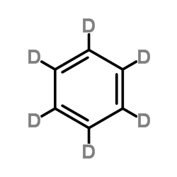 |
Benzene-d6
CAS:1076-43-3 |
|
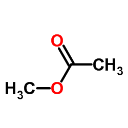 |
Methyl acetate
CAS:79-20-9 |
|
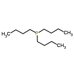 |
Tributylphosphine
CAS:998-40-3 |
|
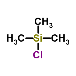 |
Chlorotrimethylsilane
CAS:75-77-4 |
|
 |
n-butylamine
CAS:109-73-9 |