A specific embedding resin (PVK) for fine cytological investigations in the photoemission electron microscope.
S Grund, J Eichberg, F Asmussen, S. Grund, J. Eichberg, F. Asmussen
文献索引:J. Ultrastruct. Res. 80(1) , 89-97, (1982)
全文:HTML全文
摘要
The photoelectric semiconductor, poly- N-vinylcarbazole (PVK) provides a specific embedding resin for studies of semi-thin sections (50 nm) in the photoemission electron microscope (PEEM). The essential advantages of PVK consist of immediate emission and a long usable observation period, so that it has become possible to study spatial associations of structures in large area semithin sections and serial sections. Using PVK, emission current densities may be reached which permit the imaging of structures without heavy metal staining. Image formation by low-energy electrons from a blocking layer (contact between semiconductor and metal) as light-sensitive site is discussed.
相关化合物
| 结构式 | 名称/CAS号 | 分子式 | 全部文献 |
|---|---|---|---|
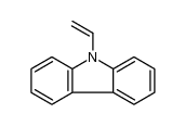 |
聚(9-乙烯咔唑)
CAS:25067-59-8 |
(C14H11N)x |
|
A facile route for the synthesis of poly(N-vinylcarbazole)/m...
2008-11-01 [J. Nanosci. Nanotechnol. 8(11) , 6031-7, (2008)] |
|
Monolithic poly(N-vinylcarbazole-co-1,4-divinylbenzene) capi...
2013-09-07 [Analyst 138(17) , 5089-98, (2013)] |
|
[The study of electroplex emission based on PVK/BCP].
2005-05-01 [Guang Pu Xue Yu Guang Pu Fen Xi 25(5) , 669-71, (2005)] |
|
Photoinduced electron transfer and hole migration along copo...
2007-04-01 [J. Nanosci. Nanotechnol. 7(4-5) , 1419-26, (2007)] |
|
Bacteriorhodopsin-based Langmuir-Schaefer films for solar en...
2003-06-01 [IEEE Trans. Nanobioscience 2(2) , 124-32, (2003)] |